A perfect crystal structure exists when all the atoms are arranged in order through the entire material. When this occurs the metal has extraordinarily high strength. However, the crystal structure is rarely perfect, and instead contains imperfections that reduce the strength. For instance, the theoretical strength of pure aluminium is about 4600 MPa whereas the actual strength is only about 100 MPa owing to imperfections in the crystal structure. As another example, the strength of pure titanium is reduced from 7300 MPa to below 200 MPa owing to lattice imperfections. The most common imperfections are point defects, dislocations and grain boundaries.
Point defects
Point defects are localised disruptions in an otherwise perfect arrangement of atoms in a crystal lattice structure. A point defect involves a single atom or pair of atoms, and thus is different from extended defects such as dislocations and grain boundaries (which are described later). Point defects occur at one or two atomic sites, but their presence is felt over much larger distances in the lattice structure. There are three main types of point defects found in metals: vacancies, interstitial defects and substitutional defects.
Vacancies
A vacancy is a point defect where an atom is missing from its normal site in the crystal structure (Fig. 4.5). The vacancy disrupts the regular arrangement of atoms, and causes a local increase in the strain energy owing to the minor misalignment in the atom positions. Vacancies in aerospace alloys are formed during solidification and processing. During cooling and solidification, the atoms, which are randomly spaced when the metal is molten, arrange themselves to form an ordered crystalline pattern at the freezing point. Not all the atomic sites are filled during freezing, which occurs over a narrow temperature range (typically less than 1 °C) and, thereby, vacancies are created. Plastic forming and shaping of the solid metal also creates vacancies. During plastic forming, the atoms are permanently displaced from the original lattice position to change the shape of the metal component. Vacancies are created by the displacement of the atoms because lattice points in the crystal structure are left unoccupied by atoms of the base metal (or substitutional element). Vacancies are also created when materials operate at high temperature (e.g. jet engine components). The concentration of vacancies is determined by many factors, with 1012 to 1016 per cubic metre being the typical range for aerospace alloys.
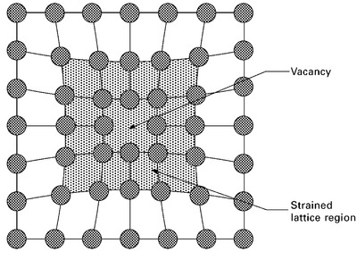
4.5 Point defect vacancy within a crystal structure. The shaded region indicates the region of high strain caused by the vacancy.
Interstitial defects
An interstitial defect is formed when a foreign (solute) atom is positioned in the crystal structure at a point that is normally unoccupied (Fig. 4.6). The defect is formed when a solute atom such as an alloying or impurity element sits within a gap between the crystal lattice points of the base metal (solvent). An interstitial atom is usually smaller than the solvent atoms located at the lattice points, but is larger than the interstitial site it occupies. Consequently, the surrounding crystal structure is distorted. An interstitial defect is often formed in metal alloys when the size of the solute atom is less than about 85% of the size of the host metal atom. In many cases, the solute atoms are less than half as small as the base metal. Carbon in iron (steel) is one example of an element that is interstitial.
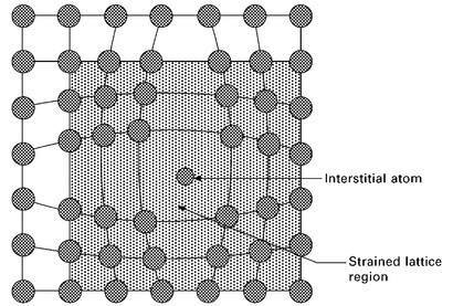
4.6 Interstitial defect within a crystal structure. The shaded region indicates the region of high strain caused by the interstitial defect.
Substitutional defects
A substitutional defect is formed when an atom from the host metal is replaced with a solute atom. Substitutional defects are created by the deliberate addition of alloying elements or the unavoidable inclusion of impurity elements. Substitutional atoms may be larger than the host atom, thus reducing the interatomic spacing in the surrounding crystal structure or the substitutional atoms can be smaller which forces the surrounding host atoms to have a greater interatomic spacing (Fig. 4.7). In either case, substitutional defects disturb the surrounding crystal structure and cause a local increase in the lattice strain energy.
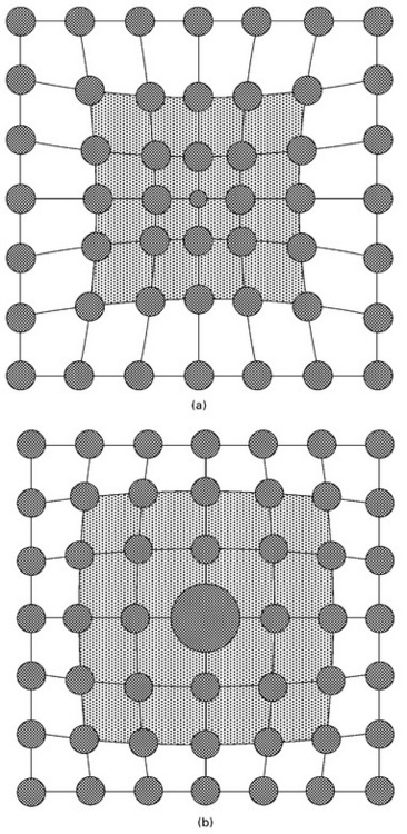
4.7 Substitutional atoms which are (a) smaller and (b) larger than the solvent atoms in the crystal structure. The shaded region indicates the region of high strain caused by the substitutional defect.
Dislocations
Dislocations are one of the most important types of lattice defects because of their strong influence on material properties such as strength, deformability, ductility and fracture toughness. Dislocations are an atomic disruption along a plane of the crystal lattice. Dislocations are known as line defects because they have a high aspect (length-to-width) ratio; being relatively long (typically several dozen to many thousand of atom spacings) and very thin (only 1 or 2 atom spacings wide). Dislocations are formed during solidification and plastic forming of metals.
Similar to point defects, dislocations are present in high concentrations in high-strength metals. Soft metals have a relatively low concentration of dislocations (typically under 106 cm of total dislocation length per cubic centimetre of material). This might seem a lot, but it is small compared with high-strength metals that contain anywhere between 1012 and 1014 cm dislocation line per cubic centimetre. If the dislocations were stacked end-to-end, then the dislocations in an aircraft panel (measuring 1.5 m long, 1.5 m wide and 3 mm thick) would extend over 1000 million km (or the distance much greater than from the sun to earth)! Such high dislocation line distances are only possible because they are packed close together (as shown in Fig. 4.8).
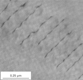
4.8 High magnification image of dislocations. (from G. Zlateva and Z. Martinova, Microstructure of metals and alloys, CRC Press, Boca Raton, 2008)
Edge dislocations
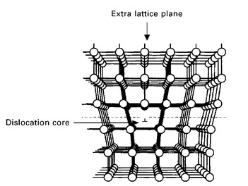
There are two types of dislocations: edge and screw. An edge dislocation can be visualised as being caused by the termination of a lattice plane in the crystal, as illustrated in Fig. 4.9. The surrounding planes are not straight, but instead bend around the edge of the terminating plane so that the crystal structure is perfectly ordered on both sides. The analogy with a stack of paper is apt. If a half sheet of paper is inserted in a stack of paper, the defect in the stack is only noticeable at the edge of the half sheet, and this is the location of the dislocation. The edge dislocation that is shown in Fig. 4.9 runs along the base of the terminated plane. Because of their structure and shape, dislocations create a local strain field in the lattice. Above the dislocation line there is a compressive strain (owing to compaction from the extra plane of atoms) and below is a tensile strain. This strain field, like the strain field surrounding point defects, is important in the strengthening of metals.
Screw dislocations
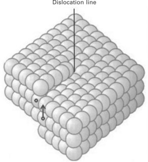
The screw dislocation can be visualised as cutting a crystal along a lattice plane and then sliding one half across the other half by an atomic spacing, as shown in Fig. 4.10. If the cut only goes part way through the crystal, and then slips, the boundary of the cut is a screw dislocation. The screw dislocation derives its name from the spiral stacking of crystal planes around the centre line.
Dislocation slip
Dislocations found in metals are a mixture of edge and screw dislocations, and both types have a large influence on the material properties when they move through the lattice structure under an external force. Dislocations are unable to move when the applied force is below the elastic limit of the metal. In elastic deformation, the shape change in the material is a result of stretching of interatomic bonds, but the force is too weak to cause dislocation motion. When the applied stress reaches the yield strength of the metal then the dislocations move by a process called slip. In fact, the yield strength is defined by the force needed to cause dislocation slip; weak forces are needed to cause dislocation slip in low-strength metals whereas stronger forces are required for higher strength materials. For instance, the applied force needed to cause dislocation slip in a high-strength steel used in aircraft landing gear (with a yield strength of about 2000 MPa) is about four times greater than for aluminium alloy used in the fuselage and wings (around 500 MPa). Dislocations also have a large influence on the plastic deformation and ductility by allowing the material to flow. Without the presence of dislocations, materials are brittle and plastic deformation is restricted.
The process of dislocation slip is represented in Fig. 4.11. When the applied force exceeds the elastic stress limit then sufficient energy exists to break the strained bonds between the metal atoms next to the dislocation. The terminated plane of atoms is forced sideways which breaks the bonds along one side of the dislocation. The ruptured bonds are immediately reformed, but on the other side of the dislocation. This shift in bonding causes the dislocation to slip sideways by one atom spacing. When the process continues by maintaining the applied force then the dislocation is able to move through the crystal. The common analogy to dislocation slip is moving a carpet along a floor by using a fold or crease that is easily pushed along its length. Another way to visualise dislocation slip is to think about how a caterpillar moves forward. A caterpillar lifts some of its legs at any given time and uses that motion to move.
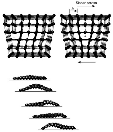
4.11 The process of dislocation slip is analogous to the motion of a caterpillar.
Dislocations move along specific lattice planes of a crystal, called slip planes. However, dislocations do not move with the same degree of ease on all the crystallographic planes. Dislocations move most easily along the lattice planes with the closest packed atoms (i.e. most dense atomic packing). The number of slip planes is determined by the crystal structure. Bcc crystals have the highest number of slip planes (48), fcc an intermediate number (12) and hcp the smallest number (3). In general, the higher the number of slip planes then the greater the strengthening effect by strain hardening. For example, work-hardened β-titanium (bcc) has a tensile strength of about 400 MPa, aluminium (fcc) 150 MPa and magnesium (hcp) 110 MPa.
Grain boundaries
Very rarely do the atoms in a crystal structure extend in straight planes for the entire length of the metal structure. In most metals, the crystals are small and are orientated in many directions, as shown in Fig. 4.12. This is known as a polycrystalline metal. A grain is a volume of the polycrystalline material within which the arrangement of the atoms is nearly identical. However, the orientation of the atoms is different from each adjoining grain. That is, the arrangement of atoms within each grain is identical, but the grains are orientated differently. The metals used in aircraft structures are polycrystalline; they contain a large number of small grains (typically tens to several hundred micrometres in size) which are randomly orientated. However, aerospace metals are sometimes manufactured by solidification and mechanical forming processes so that the grains have a preferred orientation. Jet engine turbine blades are processed under special conditions so that the metal is a single grain.
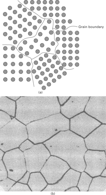
4.12 Grain structure of: (a) polycrystalline material; (b) steel. (from Metals handbook, 8th ed. Vol. 7: Atlas of microstructures of industrial alloys, American Society for Metals, Metals Park, Ohio, 1972)
The surface that separates the individual grains is called a grain boundary. The boundary is a very narrow zone (typically under two atom spacing) where the lattice structure of two adjoining grains is not aligned. Grain boundaries are important defects in controlling the strength, ductility and other material properties because they impede dislocation motion. There are two types of grain boundary, low- and high-angle boundaries, and both are found together in metals. A low-angle boundary is formed when the misorientation between adjoining grains is small enough (usually under a few degrees) to allow dislocations to slip across the boundary. A high-angle boundary occurs when the crystallographic orientation changes abruptly in passing from one grain to another. The misorientation between the grains is large enough to stop or severely restrict dislocation movement across the boundary, and for this to occur the angle must exceed 5–8°.
Leave a Reply