Since the seventeenth century, the ordinary optical microscope has been used to observe objects too small to detect with the naked eye. It uses lenses to bend visible light and create magnified images of these small structures. Its invention brought about breakthroughs in many branches of science.
However, since an electromagnetic wave can only resolve objects that are at least the size of its wavelength, an optical microscope can see details only as small as about 10-7 meters. An optical microscope could therefore never be used to observe individual atoms, whose size is about 10-10 meters. Quantum physics, however, offers other ways of peering even more deeply into nature’s depths.
Broglie demonstrated that ordinary matter also has wavelike properties. This was codifed by his simple but powerful relation λ = h⁄p. An electron, for example, accelerated fast enough can have a wavelength as small as 10-12 meters (or 100,000 times smaller than visible light). This is short enough to view objects at the atomic scale, a realization that resulted in the birth of the electron microscope. In this case, an electron beam illuminates the sample and produces a magnified image. Instead of glass lenses, the electrons must be focused by magnetic fields.

This image of an ant’s head was produced using a scanning electron microscope.
(Image courtesy of the U.S. Geological Survey)
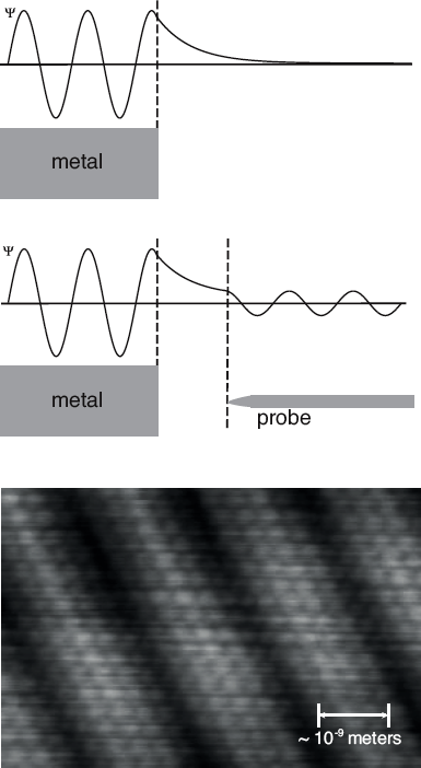
The desire to image even smaller objects led scientists to apply another aspect of quantum physics that we described namely quantum tunneling. The scanning tunneling microscope (STM) consists of a very sharp, metallic tip that is brought very close to a metallic surface and used to map its topography at the atomic scale.
Ordinarily, electrons within a metal have a lower potential energy than they would outside of the metal. The space around the metal therefore serves as a potential barrier. The wave function for an electron in a metal will leak out ever so slightly but quickly decay away to zero. However, when the metallic tip is brought near enough, and a constant voltage is applied to it, the electron can tunnel through the small, “forbidden” gap and reappear within the metallic tip. From there it flows into a circuit and is recorded as a tiny electric current drawn from the surface under study.
The probability if this happening is very sensitive to the width of the gap, so as the tip moves across the surface, the instrument can map the up-and-down features of the surface based on how much current flows. Conversely, a sensitive feedback mechanism can be used to move the position of the tip to maintain a constant current of electrons. This results in an up and down motion of the tip, tracing the silhouette of each atom in the sample. The STM can be used to map out surface features as small as 10-10 meters in width or 10-11 meters in depth. This is fine enough to image and even manipulate individual atoms within materials.

An electron wave function quickly dies away outside of a metal’s surface, unless a metal probe tip is brought nearby. In that case, electrons can tunnel through the gap, and the measured current is a sensitive probe of surface features. The STM image shows a gold surface, on which individual atoms can be seen.
(Bottom image courtesy of Erwin Rossen, Technical University Eindhoven)
The STM was first developed in 1981. So powerful were its applications that its inventors, Gerd Binnig and Heinrich Rohrer, were awarded the Nobel Prize in physics only 5 years later. This technology has since been applied to measure the flatness of surfaces, detect flaws in materials, and to monitor lubricant thickness. Is has also been used in nano-engineering to move atoms, to increase reflectivity in specialized X-ray mirrors, to improve electronic performance, and even to repair organic molecules at the atomic level.
Leave a Reply